
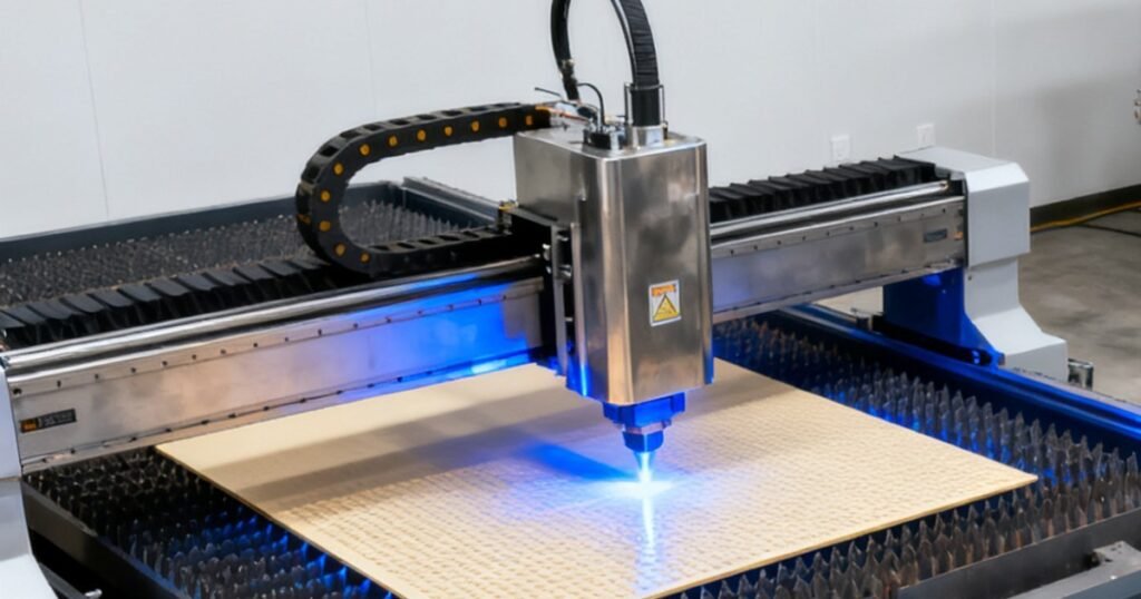
A ceramic substrate is a dense, sintered ceramic sheet that serves as the electrical insulator, mechanical carrier, and heat spreader for high-performance electronic circuits. This guide covers the five substrate materials in commercial use, standard thickness and size, the seven metallization routes, and when to choose ceramic over FR-4. It is written for engineers spec'ing a substrate for the first time, with links to fuller property data for alumina ceramic parts.
- Main materials: Al₂O₃, AlN, Si₃N₄, ZTA, BeO
- Thermal conductivity range: 10 to 300 W/m·K
- Standard thickness: 0.25 to 2.0 mm
- Metallization: DBC, DPC, AMB, LTCC, HTCC, thick film, thin film
What is a ceramic substrate?
A ceramic substrate is a fully sintered ceramic sheet used as the base of an electronic circuit or module. It carries three jobs at the same time: it insulates conductive traces from each other, it supports mounted components mechanically, and it moves heat from the die to a heat sink or baseplate. That triple role is what separates it from an organic laminate like FR-4, which insulates and supports well but conducts heat poorly.
Engineers move to a ceramic substrate when power density, operating temperature, frequency, or lifetime requirements pass a threshold that FR-4 cannot meet. The material choice, thickness, and metallization then set how well the substrate meets those requirements.
Ceramic substrate materials at a glance
Five materials cover almost every commercial ceramic substrate: aluminum oxide, aluminum nitride, silicon nitride, zirconia-toughened alumina, and beryllium oxide. Aluminum oxide is the volume default because it balances performance and cost; the others earn their premium in narrower use cases.
| Material | Thermal conductivity (W/m·K) | Dielectric constant (1 MHz) | Bending strength (MPa) | CTE (ppm/°C) |
|---|---|---|---|---|
| Al₂O₃ (95%) | 10 to 16 | 9.6 | 292 | 8.4 |
| AlN | 170 to 230 | 8.9 | 350 | 4.5 |
| Si₃N₄ | 80 to 100 | 8.7 | 812 | 2.56 |
| ZTA | 20 to 25 | 10 | 400 to 500 | 8 |
| BeO | 250 to 300 | 6.5 | 240 | 7.5 |
Aluminum oxide handles roughly 90 percent of ceramic substrate volume because its cost-to-performance ratio suits most electronic packaging, LED, and medium-power module needs. Aluminum nitride is chosen when heat, not electrics, drives the design; its thermal conductivity is roughly ten to twenty times alumina. Silicon nitride trades some thermal conductivity for very high fracture toughness, making it the AMB default for EV inverters. ZTA raises alumina's toughness at a modest thermal penalty. Beryllium oxide has the highest thermal conductivity of the group, but its powder is toxic and most modern designs avoid it. Fuller electrical data for alumina grades sits in our alumina dielectric constant hub.
Ceramic substrate vs FR-4: when to choose ceramic
FR-4 works until heat, temperature, frequency, or lifetime requirements cross a limit; ceramic substrates cost more but hold every one of those axes further out. The direct comparison shows why FR-4 remains the default for consumer and general industrial boards, and why ceramic dominates power, RF, and safety-critical hardware.
| Property | FR-4 | Ceramic (alumina) |
|---|---|---|
| Thermal conductivity (W/m·K) | 0.3 to 0.4 | 10 to 21 (up to 230 for AlN) |
| Max continuous temperature | ~130°C (Tg limit) | ≥1,000°C |
| CTE (ppm/°C, in-plane) | 14 to 17 | 7.7 to 8.4 |
| Dielectric loss at 1 GHz | ~0.02 | <0.001 |
| Relative cost | 1× | 10 to 30× |
| Lead time | Days | Weeks |
| Design condition | If yes |
|---|---|
| Power density > 1 W/mm² at the substrate face | Ceramic substrate |
| Continuous operation above 150°C | Ceramic substrate |
| Signal frequency above 5 GHz | Ceramic substrate |
| Long life or safety critical (EV, aerospace, medical) | Ceramic substrate |
| None of the above | FR-4 is likely enough |
The 10 to 30 times cost gap is why ceramic substrates are not universally adopted. When a specific requirement forces the switch, ceramic becomes a small fraction of module cost; when no such requirement exists, FR-4 remains the correct engineering choice.
Standard thickness, size, and surface finish
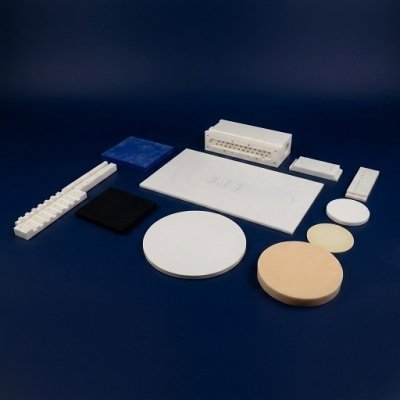
Ceramic substrates ship in a small set of standard thicknesses because tape casting, dry pressing, and cold isostatic pressing lines are tooled for them. Standard alumina substrate thickness options are 0.25, 0.38, 0.5, 0.635, 0.8, 1.0, 1.25, 1.5, and 2.0 mm, with 0.635 to 1.0 mm covering the majority of LED and power module designs.
| Thickness | Typical applications |
|---|---|
| 0.25 to 0.38 mm | Thin-film circuits, small LED modules, compact sensor packages |
| 0.5 to 0.635 mm | Standard LED boards, medium-power modules, DBC circuits |
| 0.8 to 1.0 mm | Higher-power modules, mid-voltage insulators, mechanical carriers |
| 1.25 to 2.0 mm | High-voltage substrates, wear liners, mechanically stressed parts |
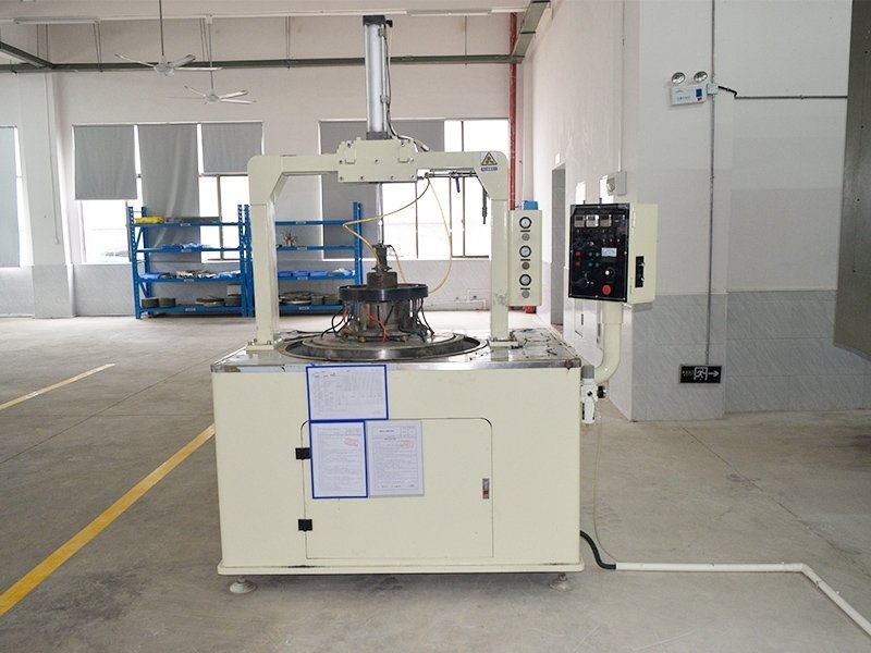
Planar sizes run from small precision coupons up to about 550 mm in the largest dimension. Surface finish is a separate spec: as-fired for setters, ground to Ra 0.4 to 0.6 μm for standard mounting, and lapped to Ra 0.1 μm for wafer chucks and thin-film metallization. Specify only the finish the function needs, since lapped area is the largest single cost driver in a substrate quote.
Metallization: how ceramic substrates become circuits
Bare ceramic is an insulator, so it becomes a functional circuit only after a metal layer is bonded on. Seven metallization routes cover the commercial market, each paired with specific substrate materials and application classes.
- DBC (Direct Bonded Copper): Copper bonded to alumina or aluminum nitride under oxygen partial pressure, delivering 0.127 to 0.4 mm copper layers for medium-power modules and LED modules.
- DPC (Direct Plated Copper): Copper electroplated on a polished ceramic surface, supporting fine features under 100 μm for LED, sensor, and small package applications.
- AMB (Active Metal Brazing): Copper brazed to silicon nitride or aluminum nitride using an active filler alloy, giving up to 1.2 mm copper and the highest thermal cycling reliability, standard for EV inverters and photovoltaic modules.
- LTCC (Low-Temperature Co-fired Ceramic): Green tapes with printed silver or gold conductors fired at 850 to 900°C, for RF and multilayer modules.
- HTCC (High-Temperature Co-fired Ceramic): Tungsten or molybdenum conductors fired at 1,300 to 1,600°C, 3 to 8 layers for aerospace and hermetic packages.
- Thick film: Screen-printed pastes fired at 600 to 900°C, the economical choice for hybrid circuits and sensor packages.
- Thin film: Sputtered metal patterned photolithographically for the highest resolution, used in precision analog and RF modules.
A supplier of bare ceramic substrates hands off to the customer's PCB house or metallization line after the ceramic ships, delivering the substrate as-fired, ground, or lapped to whatever finish the downstream process requires, with laser scribe lines and drilled holes added where the drawing calls for them.
Frequently asked questions
How does substrate thickness affect thermal and electrical performance?
Thickness sets a three-way trade-off. A thinner substrate cuts thermal resistance so heat leaves the die faster, but it also lowers the voltage the ceramic holds and makes the part fragile during solder reflow. A thicker substrate does the reverse. Standard 0.635 mm suits most LED and power control designs; 1.0 mm and above is chosen when voltage or mechanical stress demands it.
My PCB house offered 95% or 99.5% alumina. What does the electrical difference mean for my design?
The dielectric constant, loss, and resistivity all shift with purity. 95 percent alumina sits near ε 9.6 with dielectric loss around 4×10⁻⁴ and volume resistivity above 10¹³ Ω·cm, adequate for thick-film hybrid circuits and general power modules. 99.5 percent halves loss to 2×10⁻⁴ and pushes resistivity past 10¹⁴, and 99.7 percent reaches 1×10⁻⁴, which matters in RF, microwave, and precision analog work. See our alumina dielectric constant hub for the full six-grade data set.
Which metallization process (DBC, AMB, DPC) fits which substrate material?
DBC bonds copper directly to alumina or aluminum nitride under oxygen partial pressure, giving thick copper for medium-power modules. AMB adds an active brazing filler to bond copper onto silicon nitride and aluminum nitride, which DBC cannot reliably grip, and is now the standard route for EV inverters and photovoltaic modules. DPC electroplates copper on any polished ceramic surface with a fine feature limit under 100 μm, favored for LED and sensor packaging.
When is alumina not enough and I need to move to aluminum nitride or silicon nitride?
Move up when heat, not electrics, forces the change. Alumina's 10 to 21 W/m·K covers most LED and medium-power modules; once heat flux outgrows it, aluminum nitride's 170 to 230 W/m·K thermal conductivity keeps junction temperatures manageable in SiC MOSFET and IGBT modules. Silicon nitride's higher fracture toughness earns its price in EV inverters and any module that sees sharp thermal cycles, where alumina and AlN both crack over time.
Next step
Need alumina or ZTA substrates in a specific size, thickness, or with a lapped face ready for metallization? See our ceramic plates and substrates page for standard forms and thickness options. For non-standard geometries, laser scribing, drilled holes, or countersunk features, our custom ceramic parts service returns DFM feedback and a quote within 24 hours.